The Deep History of Optics at the Nikon Museum, Presented by a Nikon Fan of 15 Years!
Nikon is a world-famous camera manufacturer headquartered in Japan. You can learn about Nikon’s 100+ years of history and the various products they’ve made at the Nikon Museum located in Minato, Tokyo. The writer of this article has been a user of Nikon cameras for 15 years, and will guide you on a journey into this profound world.
*Data for this article was collected on April 19th, 2021.
Business hours mentioned are subject to change due to the circumstances of the establishment. For more details, please visit the establishment’s official homepage.
*Please avoid unnecessary outings while states of emergency are declared.
Business hours mentioned are subject to change due to the circumstances of the establishment. For more details, please visit the establishment’s official homepage.
*Please avoid unnecessary outings while states of emergency are declared.
How the History of Nikon Is Synonymous With Japan’s History of Optics
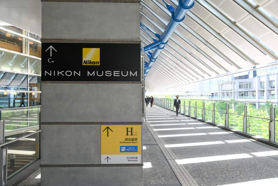
Nikon Museum is a neighbor to the company’s head office on the second floor of Shinagawa Intercity Tower C. Make your way towards Shinagawa Intercity from the pedestrian deck of the south Minato exit of Shinagawa Station and you’ll see signs that will guide you the rest of the way.
Guide display
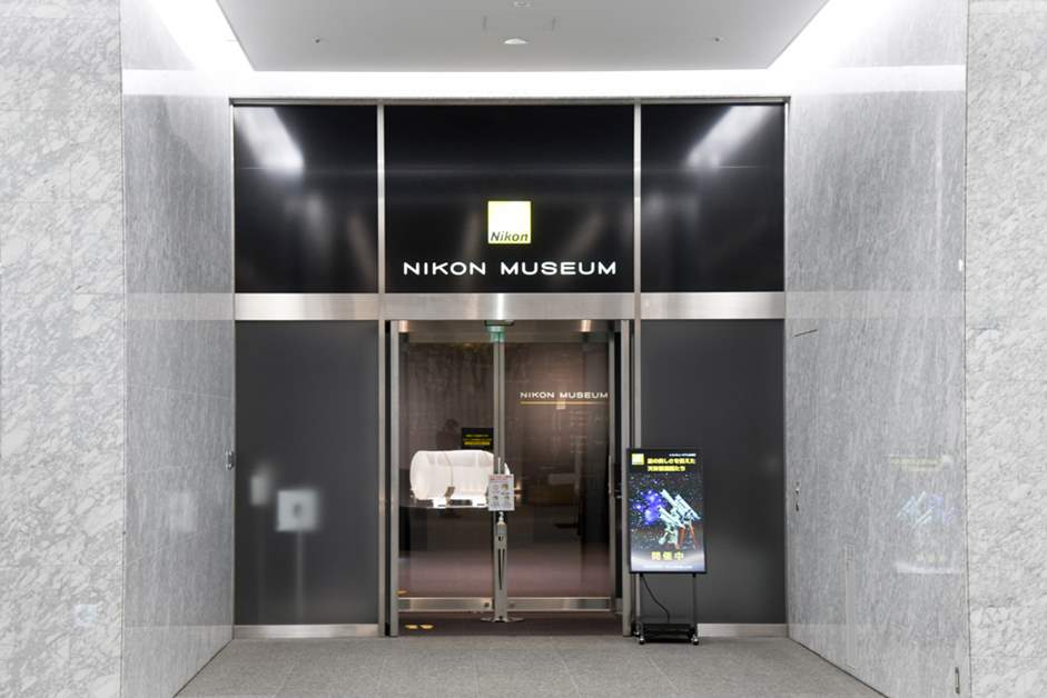
The entrance located in the skyscraper is the starting point of your journey into the world of optics. Nikon fans will be immediately delighted upon entry as they’re greeted by a poster of the Nikon F, crafted by the designer of the Nikon’s logo, Yusaku Kamekura, located just behind the reception desk.
entrance
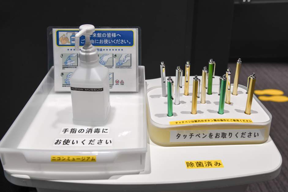
Entry to the museum is 100% free. While advance reservations are not required, visitors must register with their phone number or email address upon entry. All visitors are required to wear a mask or face covering to enter, and both hand sanitizer and styli for the touch panels are available at the entrance. Finally, touch-focused exhibits at the museum have been temporarily suspended, showing how the staff spares no effort with COVID-19 preventative measures.
Disinfectant and touch pen
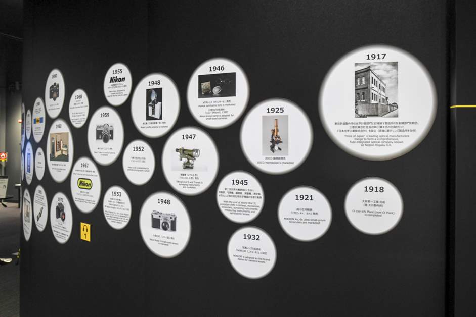
After setting foot into the museum, we first see the exhibit titled “A Century at Nikon,” a chronology of the company’s history. Nikon was founded over 100 years ago in 1917. Japan was starting down the path towards modernization at the time, and its sights were set on catching up with Germany and the US in the field of optical instruments. In order to accomplish this, Koyata Iwasaki, nephew of industrialist Yataro Iwasaki, merged three companies together into Japan Optical Industries Co., Ltd., which would eventually become the Nikon that we know today.
Full view of the building
Exhibition of "Light and Precision, 100 Years of Footprints"
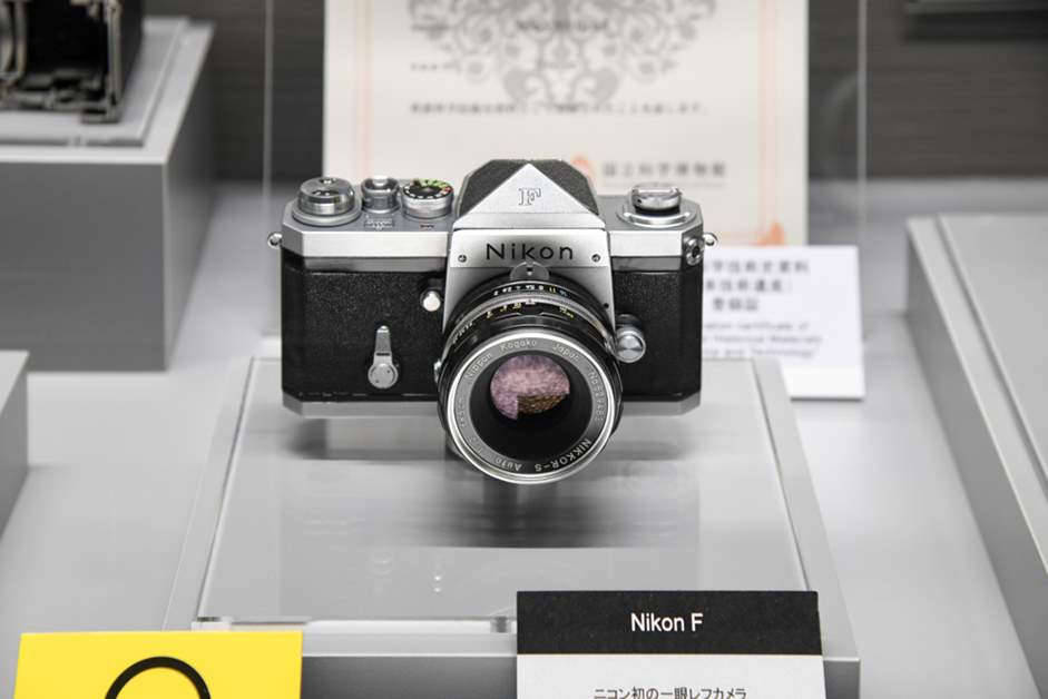
Nikon initially focused on developing optical instruments and binoculars for the military, and only after the war did the company become known by the public as a mainstream camera manufacturer. This status was further cemented in 1959 when Nikon combined all manner of cutting edge technology to launch their first lens-interchangeable SLR camera, the Nikon F.
Stand in Awe at the 850 kg Synthetic Silica Glass Ingot
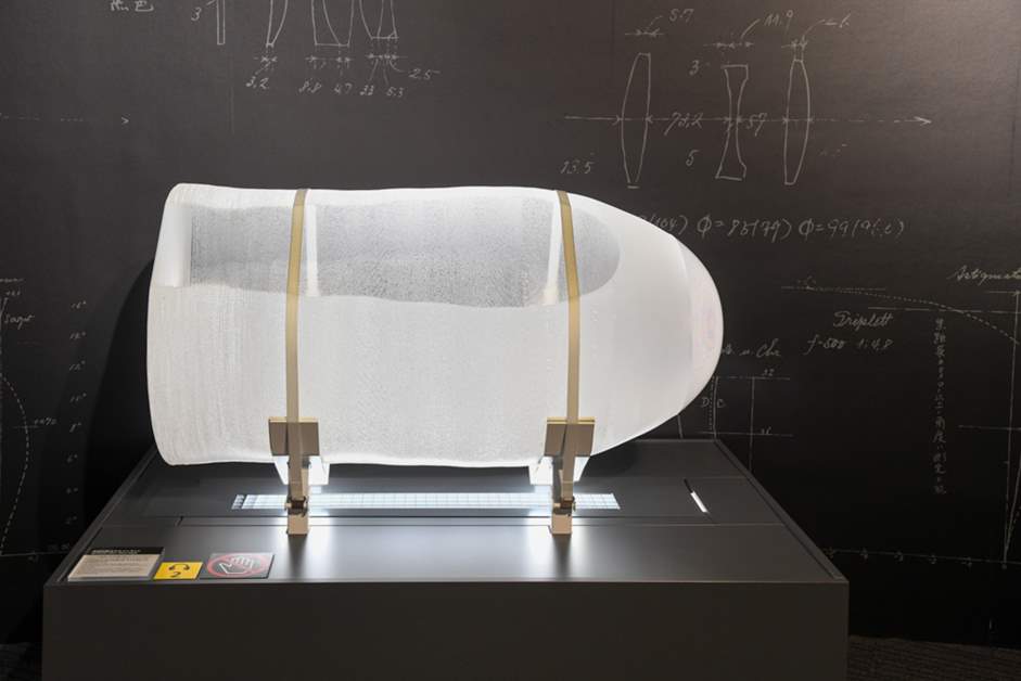
The next exhibit we see is the massive Synthetic Silica Glass Ingot, measuring 1.3 m in span and weighing in at 850 kg. These measurements alone are more than enough for one to have an understanding of how much of a treasure this ingot is. It is truly a symbol of the Nikon Museum, and glass cut from similar ingots are used for the lenses of the company’s semiconductor lithography systems. The cross section of the ingot, intentionally made visible for the purpose of the exhibit, reveals an enchanting level of transparency that seems even clearer than water. According to Vice Curator Tomoyuki Nagata, who provided commentary during my visit, only a mere handful of companies around the world would be able to produce synthetic silica glass ingot as large as the one on display in the museum.
Synthetic quartz glass ingots
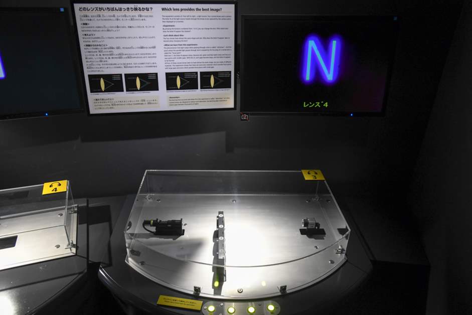
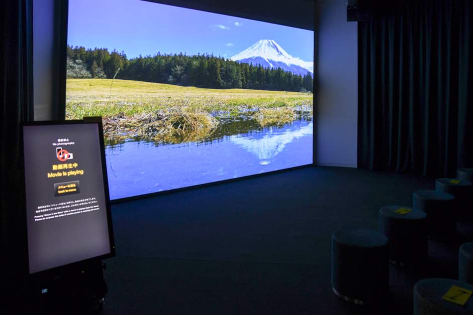
Next up is the “Lens Laboratory,” an exhibit geared towards children where you can watch videos to learn about Nikon’s history and technology, as well as have a hands-on experience as you learn about the parts of a lens. Following this exhibit is a theater with a 200 inch screen showing 4K footage of the great outdoors filmed by a drone-flown mirrorless Nikon Z 50 camera. The picturesque scenes shown are guaranteed to impress and inspire any lover of cameras.
Lens Laboratory
200-inch large screen theater
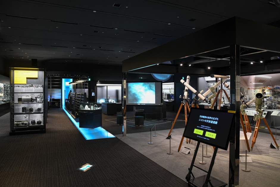
Continuing along, we have the Feature Showcase on the left of our route. One can’t help but be impressed at just how well the curators know what sorts of exhibits will make fans water at the mouth. During my visit, the featured showcase was “Astronomical Telescopes, Our Guides to the Beauty of Stars,” an exhibit featuring the various telescopes that Nikon has manufactured through the ages (on display until July 21st). Each telescope is a treasure in its own right, but leading the pack and displayed in the center is the 3-inch Telescope, the first astronomical telescope developed by Nikon in 1920 as they took a page from the Germans. By starting from the center and moving out, you can appreciate the evolution of Nikon’s telescopes.
The Jaw-Dropping Beauty of a Wall of Nikon Cameras
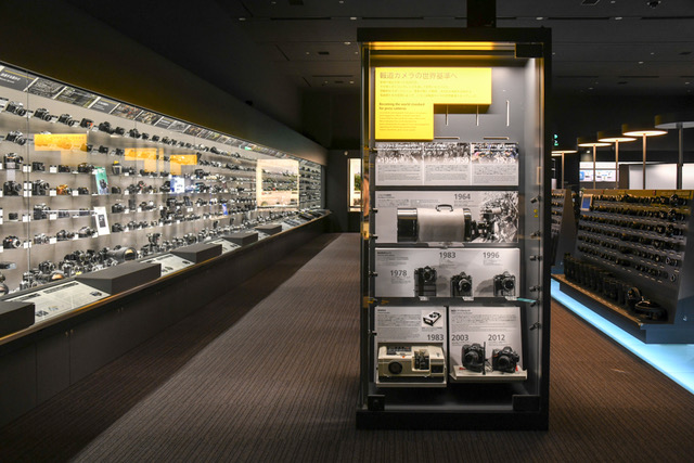
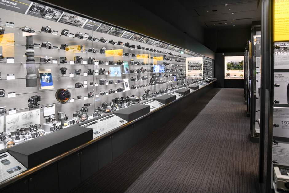
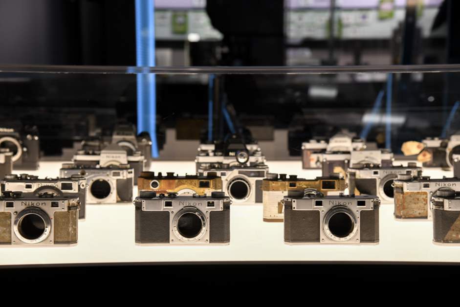
Next up are the showstopping camera exhibits. At the “Imaging” corner, you’ll find a 20 meter long glass case packed to the brim with Nikon cameras. From the historical flagship film SLR cameras F through F6 to its successor line of digital SLR cameras D1 through D6, you’ll be introduced to over 500 camera-related items presented in chronological order.
"Video and Nikon" Corner
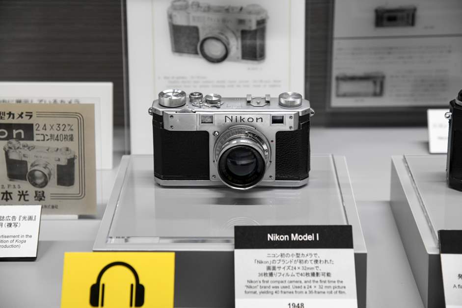
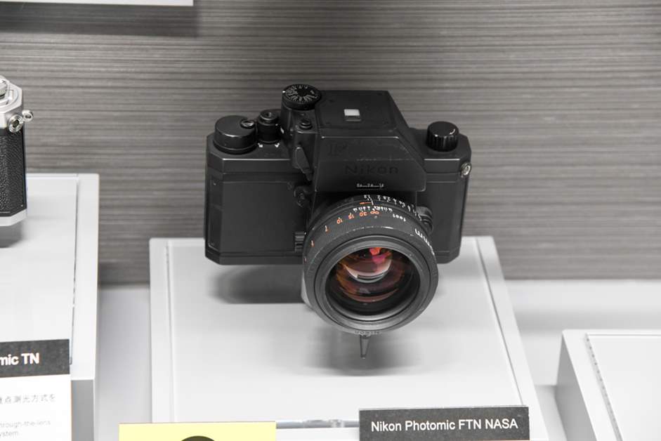
The sight of all of these Nikon cameras left me breathless. It would take forever to hear commentary about each one, so I asked Mr. Nagata about which particular three models that he’d consider to be fan favorites. His choices were the Nikon I, Nikon’s first compact camera developed in 1948, the Nikon F, Nikon’s first lens-interchangeable camera developed in 1959, and the Nikon Photomic FTN NASA, developed in 1971.
Nikon Type I
Nikon F
Nikon Photomic FTN NASA
As you can tell by its name, the Nikon Photomic FTN NASA model was a special model provided to NASA and used for the Apollo 15 mission for the fourth lunar landing. Its fully black exterior, encompassing logo and all, is designed to prevent it from reflecting onto the spaceship’s gauges and to minimize light reflecting off of the camera, while the signature lens is equipped with protuberances so that it can be operated with ease even when wearing a space suit glove.
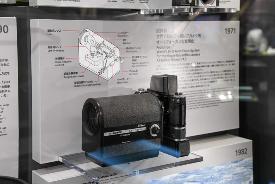
The world's first prototype lens for autofocus for SLR cameras
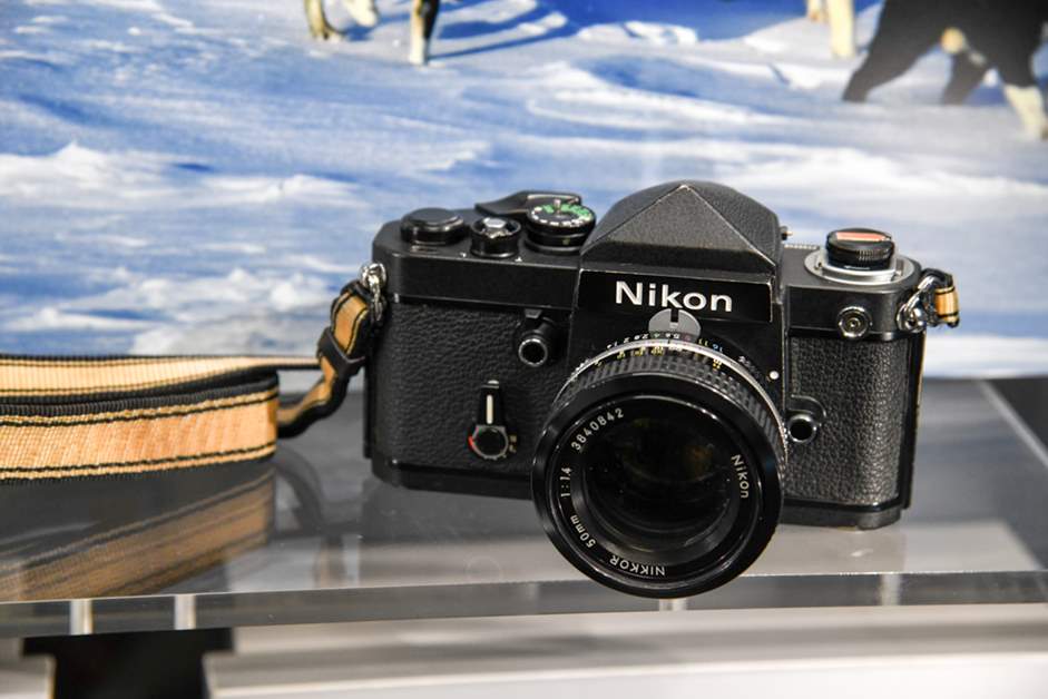
Nikon F2 Titanium Uemura Special
And of course, this exhibit has even more to offer. Displayed on a nearby shelf are “the world’s first auto focus system for an SLR camera,” “the Nikon F2 Titanium UEMURA SPECIAL designed for adventurer Naomi Uemura,” “the zoom lens boasting the longest focal length in the world, designed for being able to capture everything from the back screen to the players on home plate,” and many, many more legendary Nikon products...
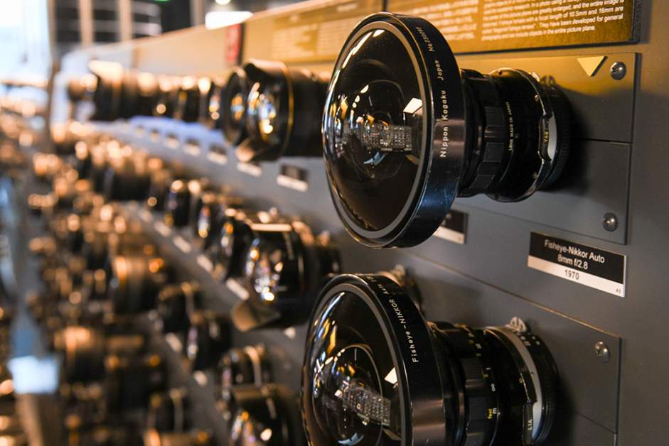
Exhibition of lenses for SLR cameras
A number of valuable prototypes born in the process of development
Next to the aforementioned cameras is a historical lineup of Nikon’s SLR camera lenses. This exhibit has so much to offer that if you were to take your time to examine each model, it would be closing time before you knew it.
The Semiconductor Lithography System, Formally Known as the Most Precise Machine
While you may feel full after taking in all those precious cameras, we’ve still only covered half of the museum. The rest of the exhibits feature Nikon technologies that the public rarely gets a chance to see, such as those used in industry or medical research.
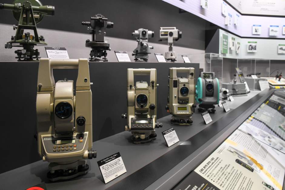
Exhibition of surveying machines
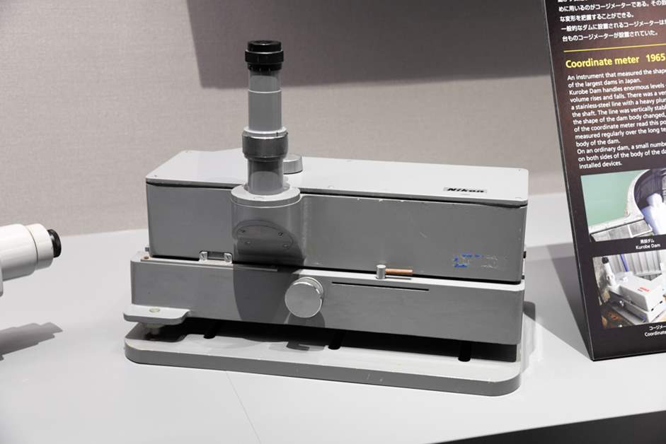
Corgimeter
For example, the measurement corner houses the “coordinate meter,”an instrument that was used to measure the shape of banks as they changed due to the volume of water stored at the famous Kurobe Dam. What seems to be just an ordinary metal box at first glance reveals a truly impressive history when you find out about it.
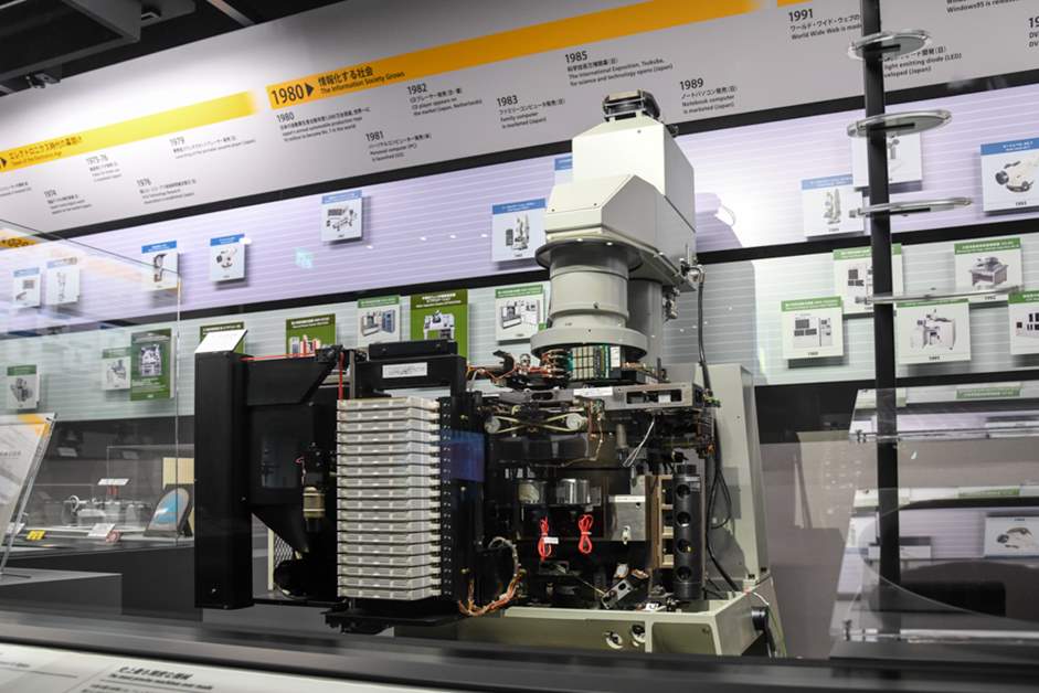
Semiconductor Exposure Equipment "NSR-1505G2A"
Right by the coordinate meter is another highlight of the Nikon Museum, the NSR-1505G2A semiconductor lithography system. A semiconductor lithography system is used to pattern intricate circuits onto silicon wafers, the base of IC and LSI. The NSR-1505G2A was built in 1984, combining cutting-edge super resolution lenses and super-high precision machine control. The model on display here isn’t actually a replica, but a real model that you can watch operate. Next to the machine is displayed the projection lens used for it, a proof of how Nikon technology was the backbone of Japan when the country took the semiconductor industry by storm.
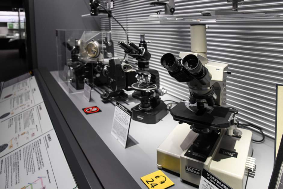
Exhibition of optical microscopes
Other products on display include models of FPD lithography systems, used in the creation of the liquid-crystal displays we see everyday on our TV and smartphone screens, the N-SIM Super Resolution Microscope, a microscope that enables the viewer to observe cell structure, the BioStation CT Cell Culture Observation System, used in iPS cell research, and more. These exhibits truly reveal just how much Nikon has contributed to various industries, from engineering and construction to the advanced research fields of medicine, biology, and even space observation.
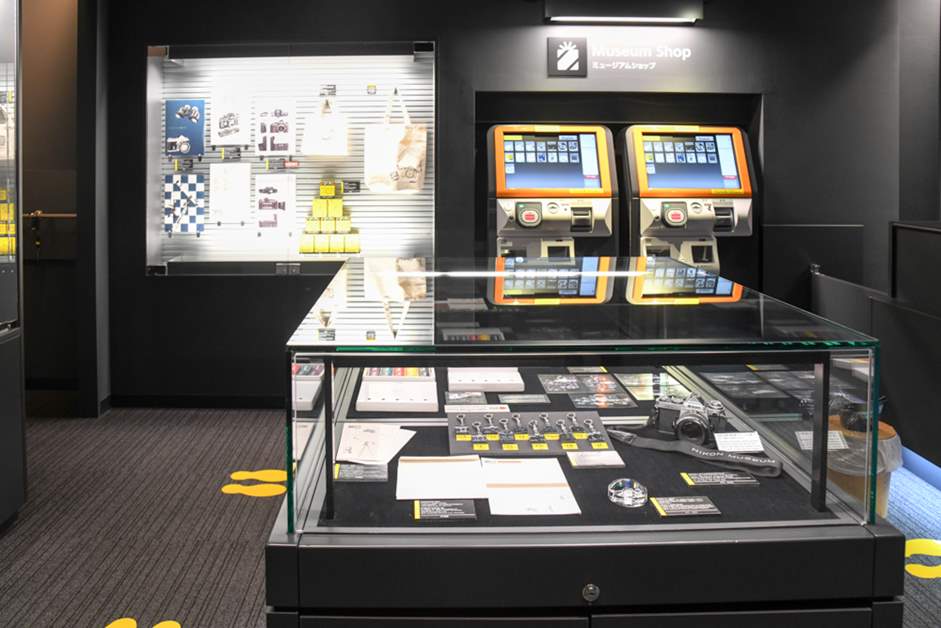
Museum Shop
Lastly, the Museum Shop is stocked with loads of great souvenirs, such as the Nikon Museum’s special design Nikon Yokan sweets. Any fan of cameras or machinery can easily spend a whole day taking in all that the Nikon Museum has to offer. I myself was unable to share even half of the content available here, so I invite you to take a visit yourself for the full experience.

